


 当前位置:
当前位置:基于MC33905设计的MCU功率管理方案
[10-10 20:38:44] 来源:http://www.88dzw.com 单片机学习 阅读:8493次
文章摘要:图4.MC33905D简化应用方框图 www.88dzw.com图9.MC33905A典型应用电路图 MC33905评估板EVBThis EVB includes two I/O test points that can be configured to be pulled up to VSup or pulled down to GND through a resistor and indicator LED. These are easily configured via jumper settings. The SBC can also be exercised in debug mod
基于MC33905设计的MCU功率管理方案,标签:单片机开发,单片机原理,http://www.88dzw.com图4.MC33905D简化应用方框图
 www.88dzw.com
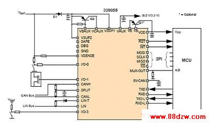
图9.MC33905A典型应用电路图
MC33905评估板EVB
This EVB includes two I/O test points that can be configured to be pulled up to VSup or pulled down to GND through a resistor and indicator LED. These are easily configured via jumper settings. The SBC can also be exercised in debug mode (watchdog re-fresh/monitoring not needed) by simply populating a jumper. Separating the input supply voltage to VSup1 and VSup2 is also made simple with a jumper configuration. Specified resistor pull-downs can be implemented on DBG and MUX pins via simple jumper configurations. The status of I/O0, I/O1, VAUX, 5V_CAN, SAFE and VDD can be visually monitored via on-board LEDs. The CAN and LIN Bus signals are provided through terminal block connectors.
An isolated terminal block connector is implemented to provide power to the evaluation board with an external DC power supply.
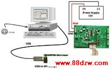
The evaluation board is operated through the graphical user interface paired up with the SPI dongle board (KITUSBSPIDGLEVME) through the 2x8 pin ribbon cable. Additionally, for added flexibility, the user can implement a custom board with a microcontroller to talk to the SBC via the 16 pin header.
MC33905评估板EVB主要特性:
•Nominal operating supply voltage range of 5.5V to 27V
•Individually routed power supply inputs for VSup1 and VSup2
•5.0 V regulator for MCU with external PNP ballast transistor to increase current capability.
•Multiple CAN Bus termination options supported via socket
•Two high/low side I/Os (SPI configurable) accessible through test points.
•Status of I/O0 and I/O1 indicated by LED (dependent on jumper configuration)
•Debug Mode/watchdog configuration via jumper settings
•MUX output voltage accessible through test point and external resistor selectable through jumper
•3.3 V or 5.0 V output voltage test point VAUX (SPI configurable)
•I_WAKE_I test point to enable a FET and load VDD with current to wake up the SBC.
•LIN1_T and LIN2_T test points to monitor I/O voltages (SPI configurable)
•I/O0, I/O1, VAUX, 5V_CAN, SAFE and VDD status indicated by LED
•100mil 2x8-pin standard header connector for SPI communication
•100mil 16-pin standard header connector for custom MCU board connection
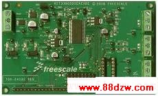
图10.MC33905评估板KIT33905D5EKEVBE外形图
 www.88dzw.com
图11.评估板KIT33905D5EKEVBE建立配置方框图
Tag:单片机学习,单片机开发,单片机原理,维修教程知识 - 单片机学习
《基于MC33905设计的MCU功率管理方案》相关文章
- › 基于MC9S08AW32和HT1621家电液晶显示系统设计
- › 基于MCU和FPGA灵活设计车载信息娱乐系统
- › 基于MCU设计的离线锂电池充电器
- › 基于MCF51EM256设计的多相智能电表技术
- › 基于MC33905设计的MCU功率管理方案
- › 基于MCF51QE128的SD卡接口设计
- 在百度中搜索相关文章:基于MC33905设计的MCU功率管理方案
- 在谷歌中搜索相关文章:基于MC33905设计的MCU功率管理方案
- 在soso中搜索相关文章:基于MC33905设计的MCU功率管理方案
- 在搜狗中搜索相关文章:基于MC33905设计的MCU功率管理方案
最新更新