


 当前位置:
当前位置:SST89C58电子盘电路及代码
[10-10 20:38:44] 来源:http://www.88dzw.com 微机|单片机 阅读:8488次
文章摘要:Reference design for SST ATA-Disk Chip into 8051 microcontrollerApplication noteAbstract: this application note introduces the hardware and firmware of reference design for SST ATA-Disk Chip SST58SD/LDxxx into SST FlashFlex51 SST89C54/58 (8051 compatible microcontroller).1.Hardware connections:Pleas
SST89C58电子盘电路及代码,标签:电路设计,http://www.88dzw.com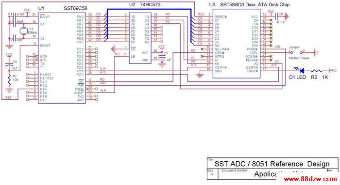
Reference design for SST ATA-Disk Chip into 8051 microcontroller
Application note
Abstract: this application note introduces the hardware and firmware of reference design for SST ATA-Disk Chip SST58SD/LDxxx into SST FlashFlex51 SST89C54/58 (8051 compatible microcontroller).
1.Hardware connections:
Please reference to attached schematic diagram for hardware connections.
SST ATA-Disk Chip (ADC) SST58SD/LDxxx only supports one working mode, ie. ATA/IDE mode, all control signals are connected based on Table 2-8, Page 14 on datasheet. After executed Set Feature Command to enable 8-bit data transfers, all higher 8 bit data bus ( D8-D15) are don’t care and can be No Connect. RESET# (pin1) is optional, it can be tied up to Vcc if not used. After power-up, ADC will automatically be reset internally, it doesn’t need external reset input. But it’s a good practice to connect RESET# to one of I/O pins such as P1.4, in case ADC is out of control for any unknown reasons, host MCU has capability to reset ADC. DASP# is connected to an emitting diode through a resistor to Vcc, LED provides user a visibility of ADC’s internal operation. When ADC is active busy on operation, LED will be on. Please be noted that master/slave selection at CSEL pin won’t take effect until Next reset, in other words, if you change the jumper setting of master/slave selection, you MUST reset ADC once.
Ifyour application system expands any other I/O or data memory, please modify the reference design: (1)change CS3FX# to Vcc, (2)connect the output of address decoder to CS1FX#.When both CS1FX#and CS3FX# are high,ADC is de-selected and be standby state, all data bus are in high-z. When CS1FX# is low, ADC is selected and be operational. So CS1FX# acts as Chip Select (/CS) in most common peripherals.
2.Firmware design guide:
It’s important to know that ATA/IDE standard doesn’t permit access only one byte at a time to its media such as HDD or ADC, firmware must read or write data sector by sector, 1 sector has 512 bytes of data,system design engineer must design data buffer to support random access to ADC. Reference design uses the secondary block (4Kbytes x 8bit) of on-chip flash in SST89C54/58 as data buffer.
After power-up or external reset, ADC is default to be 16-bit operation. As SST89C54/58 is 8-bit MCU, firmware must enable 8-bit operation by Set Features Command, please reference to page 32 on datasheet.
If ADC is set as Slave, other than Master, you need to change the bit4 in Drive/Head Register to be 1 when writing Command to ADC, see page 17 on datasheet.
After power-on or reset,ADC will be ready to read / write operation after 200ms (typical), 500ms (maximum), see page 1 under Start Up Time in Features on datasheet.
3.Conclusion:
It’s easy to modify this reference design to any other embedded controllers as long as you follow above design guidelines.
4.Schematic diagram:
5.8051 Source code:
; all commands supported by ADC.
《SST89C58电子盘电路及代码》相关文章
- › 使用SST89C58控制单片电子硬盘的硬件电路
- › SST89C58电子盘电路及代码
- › 用SST89E564制作51仿真器
- › 用SST89C53制作的51单片机仿真器
- › 用SST89C58控制单片电子硬盘的硬件电路
- 在百度中搜索相关文章:SST89C58电子盘电路及代码
- 在谷歌中搜索相关文章:SST89C58电子盘电路及代码
- 在soso中搜索相关文章:SST89C58电子盘电路及代码
- 在搜狗中搜索相关文章:SST89C58电子盘电路及代码