


 当前位置:
当前位置:DS1670便携式系统控制器-DS1670 Portable
[09-13 17:03:21] 来源:http://www.88dzw.com 控制技术 阅读:8204次
文章摘要:Microprocessor MonitorThe microprocessor monitor circuitry of the DS1670 provides three basic functions: A precision temperature-compensated reference and comparator circuit monitors the status of VCC. When an out-of-tolerance condition occurs, an internal power fail signal is generated which forces
DS1670便携式系统控制器-DS1670 Portable,标签:计算机控制技术,工厂电气控制技术,http://www.88dzw.comMicroprocessor Monitor
The microprocessor monitor circuitry of the DS1670 provides three basic functions:- A precision temperature-compensated reference and comparator circuit monitors the status of VCC. When an out-of-tolerance condition occurs, an internal power fail signal is generated which forces the reset to the active state. When VCC returns to an in-tolerance condition, the reset signals are kept in the active state for 250 ms to allow the power supply and processor to stabilize.
- Pushbutton reset control: The DS1670 debounces a pushbutton input and guarantees an active reset pulse width of 250 ms.
- Watchdog timer: The DS1670 has an internal timer that forces the reset signals to the active state if the strobe input is not driven low prior to watchdog time-out.
Analog-to-Digital Converter
The DS1670 also provides a 3-channel 8-bit successive approximation analog-to-digital converter. The converter has an internal 2.55 volt (typical) reference voltage generated by an on-board band-gap circuit. The A/D converter is monotonic (no missing codes) and has an internal analog filter to reduce high frequency noise.An A/D conversion is the process of assigning a digital code to an analog input voltage. This code represents the input value as a fraction of the full scale voltage (FSV) range. Thus the FSV range is then divided by the A/D converter into 256 codes (8 bits). The FSV range is bounded by an upper limit equal to the reference voltage and the lower limit, which is ground. The DS1670 has a FSV of 2.55V (typically) which provides a resolution of 10 mV. An input voltage equal to the reference voltage converts to FFh while an input voltage equal to ground converts to 00h. The relative linearity of the A/D converter is ±0.5 LSB.
The analog input (AIN0, AIN1, or AIN2) for an analog-to-digital conversion is selected by the condition of the Analog Input Select (AIS) bits in the Control Register. Conversions occur every 10 ms and the result is placed in the ADC Register.
Typical Application
Figure 3 illustrates a typical application using the DS1670. In this application, the DS1670 is shown interfacing with a 386EX or 80186 microprocessor (microprocessors designed with embedded applications in mind). Communication between the microprocessor and the DS1670 is accomplished easily through three port pins (P1.0-P1.2) which are connected to the 3-wire serial interface pins of the DS1670 Serial Clock (SCLK), Chip Select (active-low CS), and serial input/output (I/O). This serial interface provides access to the real time clock, ADC, control, and status registers of the DS1670.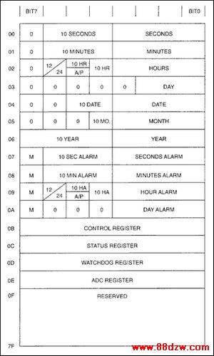
Figure 3. DS1670 address map.
Nonvolatile SRAM Control
The DS1670 also provides nonvolatile control of external SRAMs in this circuit example. The Chip Select (active-low CS), Byte High Enable (active-low BHE), and Byte Low Enable (active-low BLE) outputs of the microprocessor are gated through the DS1670 to its Chip Enable Output Low (active-low CEOL) and chip Enable Output High (active-low CEOH) output pins. The active-low CEOL and CEOH pins can be driven to the active state only when VCC is within nominal limits (>2.88V) thus preventing the system from receiving or writing corrupted data. Note that the structure of the SRAM access controller allows the microprocessor to access data in worldwide format (16 bits wide by enabling active-low CEOL and active-low CEOH simultaneously) or byte-wide format (8-bit wide by enabling either active-low CEOL or active-low CEOH).
Tag:控制技术,计算机控制技术,工厂电气控制技术,控制技术
《DS1670便携式系统控制器-DS1670 Portable》相关文章
- › 驱动器和通信电路引脚及主要特性DS1692/3692 三态差动线驱动器
- › 驱动器和通信电路引脚及主要特性DS1691A/3691 RS-422/423驱动器
- › 驱动器和通信电路引脚及主要特性DS1687/3687 负电压延迟驱动器
- › 驱动器和通信电路引脚及主要特性DS1649/3649六进制三态TTL-MOS驱动...
- › 驱动器和通信电路引脚及主要特性DS1648/3648三态TTL-MOS多路转换器...
- › 驱动器和通信电路引脚及主要特性DS1631/2/3/4、DS3631/2/3/4 驱动...
- 在百度中搜索相关文章:DS1670便携式系统控制器-DS1670 Portable
- 在谷歌中搜索相关文章:DS1670便携式系统控制器-DS1670 Portable
- 在soso中搜索相关文章:DS1670便携式系统控制器-DS1670 Portable
- 在搜狗中搜索相关文章:DS1670便携式系统控制器-DS1670 Portable
分类导航
最新更新